Energy Level Modulation in Diboron Modified SnO2 for High Efficiency Perovskite Solar Cells
中文 / Bilingual · English version
Energy level modulation in diboron modified ${\mathrm{{SnO}}}_{2}$ for high efficiency perovskite solar cells
Nengxu Li, Xiuxiu Niu, Fengtao Pei, Huifen Liu, Yang Cao, Yuquan Liu, Haipeng Xie,
Yongli Gao, Qi Chen, Fanyang Mo*, Huanping Zhou*
N. Li, F. Pei, H. Liu, Prof. H. Zhou
Beijing Key Laboratory for Theory and Technology of Advanced Battery Materials & Key
Laboratory of Polymer Chemistry and Physics of Ministry of Education
Department of Materials Science and Engineering
College of Engineering
Peking University
Beijing 100871, P. R. China
happy
happy
X. Niu, Prof. Q. Chen
Department of Materials Science and Engineering
Beijing Institute of Technology
Beijing 100081, P. R. China
Y. Cao, Prof. F. Mo
Department of Energy and Resources Engineering
College of Engineering
Peking University
Beijing 100871, P. R. China
Y. Liu, H. Xie, Prof. Y. Gao
Hunan Key Laboratory for Super-microstructure and Ultrafast Process
This article has been accepted for publication and undergone full peer review but has not been through the copyediting, typesetting, pagination and proofreading process, which may lead to differences between this version and the Version of Record. Please cite this article as doi: 10.1002/solr.201900217
This article is protected by copyright. All rights reserved
Collage of Physics and Electronics
Central South University
Changsha, Hunan 410012, P.R. China.
Abstract
Energy level modulation between perovskite and carrier transport layers to obtain a promoted carrier extraction and reduced charge recombination is an effective way for high efficiency perovskite solar cells. Here, we employ diboron as an effective interfacial modifier between ${\mathrm{{SnO}}}_{2}$ and perovskite. By taking advantage of the higher Femi level on the surface of ${\mathrm{{SnO}}}_{2}$ after diboron treatment, we obtain a power conversion efficiency of 22.04% in a solar cell device based on two-step solution processed planar n-i-p structure. With the help of thorough characterizations, we argue that the diboron treated ${\mathrm{{SnO}}}_{2}$ possesses some ${\mathrm{{Sn}}}^{3 + }$ species, which serve as electron donors with more n-type nature, promoting electron extraction and reducing carrier recombination in ETL/perovskite interface. Further analysis speculate that the formation of surface diboron-oxygen Lewis pair induces a reducing state of diboron complexes, resulting the spontaneous electron redistribution and the formation of ${\mathrm{{Sn}}}^{3 + } - {\mathrm{O}}^{ - }$ species. This provides an effective chemical approach to tune the energy alignment between the oxide ETL and absorber.
1. Introduction
In recent years, organic-inorganic halide perovskites have emerged as exciting new materials for optoelectronic devices such as solar cells ${}^{\left\lbrack 1\right\rbrack }$ , light emitting diodes (LEDs) ${}^{\left\lbrack 2\right\rbrack }$ , and photodetectors ${}^{\left\lbrack 3\right\rbrack }$ , mainly due to their remarkable properties, such as strong light absorption ${}^{\left\lbrack 4\right\rbrack }$ , superb charge carrier mobility ${}^{\left\lbrack 5\right\rbrack }$ , and low-cost fabrication ${}^{\left\lbrack 6\right\rbrack }$ . Power conversion efficiency (PCE) of perovskite solar cells (PSCs) have risen from 3.8% to a certified 24.2% ${}^{\left\lbrack 4,7\right\rbrack }$ , which is close to the state-of-the-art crystalline silicon (c-Si) solar cells. In the context of PCE, earlier work focus on the perovskites film quality, including component engineering ${}^{\left\lbrack 1c\right\rbrack }$ , fabrication optimization ${}^{\left\lbrack 8\right\rbrack }$ , and defects passivation ${}^{\left\lbrack 9\right\rbrack }$ . Meanwhile, the carrier transport layers (CTLs) are also intensively investigated. Taking the planar n-i-p PSCs as an example, tin dioxide (SnO ${}_{2}$ ) is widely used as electron transport layer (ETL) due to its high bulk mobility (up to ${240}{\mathrm{\;{cm}}}^{2} \; {\mathrm{V}}^{-1}\;{\mathrm{\;s}}^{-1}$ ) and suitable energy level ${}^{\left\lbrack {10}\right\rbrack }$ , 2,27,7’-tetrakis(N, N-di-p-methoxyphenylamine)-9,9’-spirobifluorene (spiro-OMeTAD) is one of the most adaptable hole transport layer (HTL) thanks to its suitable highest occupied molecular orbital (HOMO) energy level, excellent hole-extraction and transportation ability [11]. In addition, the interface between perovskite/ETL and perovskite/HTL are also crucial to the carrier extraction and transportation ${}^{\left\lbrack {12}\right\rbrack }$ . On one hand, the interface often induce defect formation and migration ${}^{\left\lbrack {13}\right\rbrack }$ , which lead to the observed current-voltage hysteresis and long-term device instability ${}^{\left\lbrack {14}\right\rbrack }$ . On the other hand, energy level mismatching at the interfaces will lead to non-effective charge carrier injection and excess recombination due to the carrier accumulation ${}^{\left\lbrack {15}\right\rbrack }$ . How to reduce the defects existed at the interface, and obtain a more favourable energy level alignment between perovskite and carrier transport layer are urgently needed to obtain better optoelectronic properties of PSCs.
Both defects passivation and energy level alignment at the interface have been reported in recent work. For example, organic halide salt phenethylammonium iodide (PEAI) are formed on the perovskite surface to boost the efficiency of PSCs, which may passivate the iodine vacancy defects existed at the perovskite/HTL interface ${}^{\left\lbrack {16}\right\rbrack }$ ; Poly(vinylcarbazole) (PVCz)/[6,6]-phenyl-C61-butyric acid methyl ester (PCBM) are also used as interfacial passivation layer between perovskite and ${\mathrm{{TiO}}}_{2}$ , suppressing the carrier recombination at ${\mathrm{{TiO}}}_{2}$ /perovskite interface ${}^{\left\lbrack {17}\right\rbrack }$ . In addition, some strategies are also explored to modulate the Femi-level $\left( {\mathrm{E}}_{\mathrm{F}}\right)$ of ${\mathrm{{SnO}}}_{2}$ , such as using ethylene diamine tetraacetic acid (EDTA) treated ${\mathrm{{SnO}}}_{2}$ to obtain a better energy match with the conduction band of perovskite, eliminating the charge accumulation at the perovskite/ETL interface ${}^{\left\lbrack {18}\right\rbrack }$ . Moreover, a compositional gradient modulation at the rear interface between the perovskite and HTLs can improve the hole collection and reduce charge recombination, resulting a higher efficiency PSCs ${}^{\left\lbrack {19}\right\rbrack }$ . All the optimization indicate that the defects elimination and energy level modulation of CTLs/perovskite interface are the effective means to obtain high efficiency solar cells, although the profound mechanism of energy band modification between ${\mathrm{{SnO}}}_{2}$ and perovskite is still not clear.
Here we report an effective interface engineering approach by using the diboron $\left( {{\mathrm{B}}_{2}{\mathrm{{Cat}}}_{2}}\right)$ as the interfacial modifier between ${\mathrm{{SnO}}}_{2}$ and perovskite. Based on the ${\mathrm{B}}_{2}{\mathrm{{Cat}}}_{2}$ treatment, we obtain a higher ${\mathrm{E}}_{\mathrm{F}}$ on the surface of ${\mathrm{{SnO}}}_{2}$ (meaning a more n-type nature), resulting a better energy matching at ETL/perovskite interface and a higher PCE of 22.04% with negligible hysteresis in planar n-i-p perovskite solar cells. The most visible improvement is found to be open-circuit voltage (Voc), which is mainly due to the higher carrier extraction and suppressed charge recombination at the ${\mathrm{{SnO}}}_{2}$ /perovskite interface. More importantly, we demonstrate that the ${\mathrm{B}}_{2}{\mathrm{{Cat}}}_{2}$ treated ${\mathrm{{SnO}}}_{2}$ possesses some ${\mathrm{{Sn}}}^{3 + }$ species, acting as electron donors to obtain a more n-type nature of ETLs. Finally, we speculate that the formation of surface diboron-oxygen Lewis pair induces a reducing state of diboron complexes, which further enables spontaneous electron redistribution for the formation of ${\mathrm{{Sn}}}^{3 + } - {\mathrm{O}}^{ - }$ species on the surface of ${\mathrm{{SnO}}}_{2}$ . This strategy could be extended to other similar molecules that can be used in optoelectronic devices. those for the BSO film are -7.93 eV and -4.14 eV, respectively, which are in agreement with previous report ${}^{\left\lbrack {20}\right\rbrack }$ . Although SO and BSO films exhibit the similar band structure, the BSO film shows a more n-type nature with the higher ${\mathrm{E}}_{\mathrm{F}}$ , which means its energy level matched well with perovskite materials, facilitating the electron extraction ability of ${\mathrm{{SnO}}}_{2}{}^{\left\lbrack {21}\right\rbrack }$ . In addition, the ${\mathrm{E}}_{\mathrm{F}}$ , VBM, Eg of perovskite film which fabricated by a typical two-step solution process are shown in Figure 1c, and the corresponding band structure is shown in Figure 1b. Compared the ${\mathrm{E}}_{\mathrm{F}}$ of perovskite, $\mathrm{{SO}}$ and $\mathrm{{BSO}}$ , the smaller gap between perovskite and $\mathrm{{BSO}}$ indicates the better band alignment between them and less energy loss while transporting carriers. As a result, ${\mathrm{B}}_{2}{\mathrm{{Cat}}}_{2}$ modified ${\mathrm{{SnO}}}_{2}$ , as an excellent n-type semiconductor, are more suitable to be the ETL of PSCs. of substrate that can influence the grain size of perovskite ${}^{\left\lbrack {21}\right\rbrack }$ , we therefore measured the contact angle of N, N-Dimethylformamide (DMF) on the top of the SO and BSO films. The obtained values are ${8}^{ \circ }$ for SO and ${28}^{ \circ }$ for BSO film, respectively, as shown in Figure S2, Supporting Information. This implies that the BSO film has lower wettability of DMF solvent, thus fewer nucleation sites are possessed, resulting in a reduced nucleation rate during perovskite formation. Hence, by fixing the growth rate, the slower nucleation rate based on BSO substrate results in a relatively larger grain size in the perovskite film, which is consistent with other reports ${}^{\left\lbrack {22}\right\rbrack }$ .
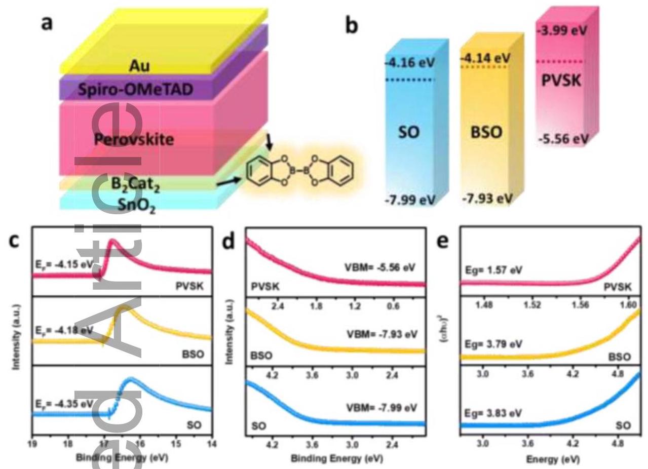
Figure 1. a) Device structure of ${\mathrm{B}}_{2}{\mathrm{{Cat}}}_{2}$ modified planar-heterojunction PSCs. b) Energy band diagram of ${\mathrm{{SnO}}}_{2}$ (SO), ${\mathrm{B}}_{2}{\mathrm{{Cat}}}_{2}$ treated ${\mathrm{{SnO}}}_{2}$ (BSO) and perovskite (PVSK) thin films. c) The secondary electron cut-off region of ultraviolet photoelectron spectroscopy (UPS) spectra of SO, BSO and PVSK films. d) The valence band region of UPS spectra of SO, BSO and PVSK films. e) The relationship of (dn) ${}^{2}$ vs energy for SO, BSO and PVSK films.
The planar heterojunction PSCs are used in this study, whose device structure is tin-doped indium oxide (ITO)/ ${\mathrm{{SnO}}}_{2}/{\mathrm{B}}_{2}{\mathrm{{Cat}}}_{2}/$ perovskite/Spiro-OMeTAD/Au (Figure 1a). When the ${\mathrm{{SnO}}}_{2}$ thin film is treated with ${\mathrm{B}}_{2}{\mathrm{{Cat}}}_{2}$ (for convenience, we denote it as BSO, detailed fabrication methods see the Supporting Information), the Fermi level $\left( {\mathrm{E}}_{\mathrm{F}}\right)$ of BSO shows an obvious up-shift compared to the reference (untreated ${\mathrm{{SnO}}}_{2}$ , we denote it as SO), as shown in Figure 1c. It can be found that the ${\mathrm{E}}_{\mathrm{F}}$ of the SO and BSO are -4.35 and -4.18 eV, respectively. In addition, the corresponding valence band maximum (VBM) are located at 3.64 and ${3.75}\mathrm{{eV}}$ below the ${\mathrm{E}}_{\mathrm{F}}$ (Figure 1d), respectively. In combination with the band gap (Eg) acquired from the UV-visible spectra (Figure 1e, 3.83 eV for SO, 3.79 eV for SBO), we then obtain the energy levels of the SO and BSO samples which are shown in Figure 1b. The VBM and conduction band minimum (CBM) of SO film are -7.99 eV and -4.16 eV, while
This article is protected by copyright. All rights reserved
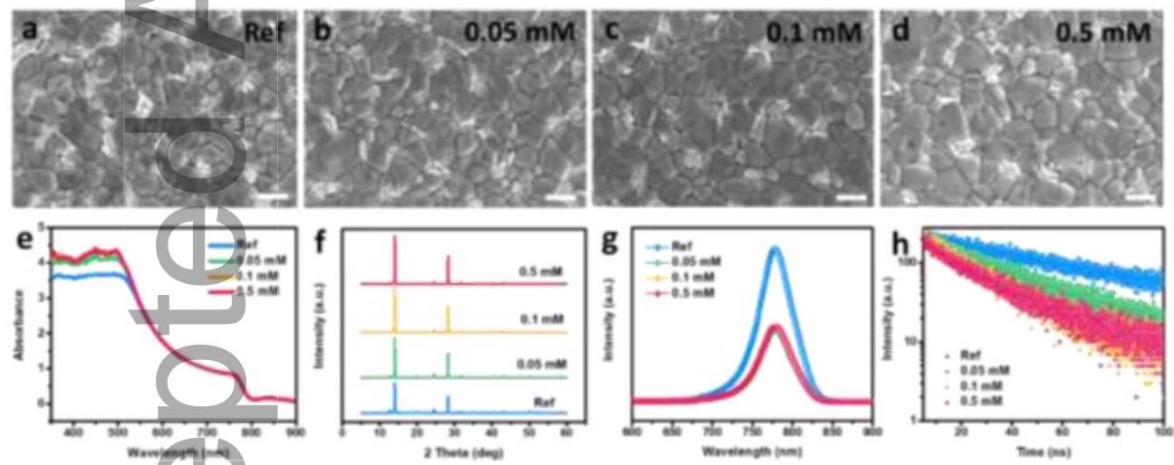
Figure 2. a, b, c, d) The top-view field emission scanning electron microscopy (FE-SEM) images; e) The UV-visible absorption spectra; f) The X-ray diffraction (XRD) patterns; g) The steady-state photoluminescence (PL) spectra; h) The time-resolved photoluminescence (TRPL) spectra of perovskite films which fabricated on $0,{0.05}\mathrm{{mM}},{0.1}\mathrm{{mM}},{0.5}\mathrm{{mM}}{\mathrm{B}}_{2}{\mathrm{{Cat}}}_{2}$ treated ${\mathrm{{SnO}}}_{2}$ films, respectively. The scale bar of SEM images is ${1\mu }\mathrm{m}$ .
As the ${\mathrm{B}}_{2}{\mathrm{{Cat}}}_{2}$ is treated on the top of ${\mathrm{{SnO}}}_{2}$ , we then attempted to understand how the BSO film affects the properties of perovskite films. To investigate this, the top-view field emission scanning electron microscopy (FE-SEM) measurement on the sample are firstly performed. It can be found that BSO based perovskite films exhibit slightly larger grain size than that of reference (SO based perovskites), regardless of the concentration of ${\mathrm{B}}_{2}{\mathrm{{Cat}}}_{2}$ , as shown in Figure 2a-d. While the morphology of ${\mathrm{{SnO}}}_{2}$ and ${\mathrm{B}}_{2}{\mathrm{{Cat}}}_{2}$ treated ${\mathrm{{SnO}}}_{2}$ have no significant difference (Figure S1, Supporting Information). In consideration of the wettability
In addition, UV-visible spectra of the SO and BSO film fabricated on ITO-glass is displayed in the Figure S3, Supporting Information. The transmittance of them are almost the same, indicating that ${\mathrm{B}}_{2}{\mathrm{{Cat}}}_{2}$ has no extra self-absorbance. The absorbance of the perovskite films which fabricated on SO/BSO are also measured, as shown in Figure 2e, confirming that ${\mathrm{B}}_{2}{\mathrm{{Cat}}}_{2}$ treatment has no significant optical influence on perovskite films. X-ray diffraction (XRD) patterns of perovskites are displayed in Figure 2f, and the peak intensity of perovskite phase is enhanced by increasing the concentration of ${\mathrm{B}}_{2}{\mathrm{{Cat}}}_{2}$ , mainly due to the larger grain size induced by BSO based substrate. Moreover, neither shifts in the peaks, nor new peaks are observed in the XRD patterns (Figure S4, Supporting Information), indicating that BSO substrate does not alter the crystal structure of the perovskite films. We further performed the Fourier-transform infrared spectroscopy (FTIR) measurements to detect the diboron species. The result is shown in Figure S5, Supporting Information. When taking diboron powder as a reference, diboron thin film which deposited on quartz substrate and annealed at ${70}^{ \circ }\mathrm{C}$ for 5 min also exhibit similar signals. This results demonstrate the existence of diboron species after annealing process, which may play an important role on the interfacial modification.
To clearly compare the electron extraction ability of SO and BSO film, we further performed the steady-state photoluminescence (PL) and time-resolved photoluminescence (TRPL) measurements (Figure 2g-h) based on the samples structure: ITO/SO/perovskite or ITO/BSO/perovskite. The PL intensity of BSO based perovskite is reduced significantly compared to SO based perovskite, ascribed to the more efficient extraction of photo-generated electrons from the perovskite to the ${\mathrm{{SnO}}}_{2}{}^{\left\lbrack {23}\right\rbrack }$ . In addition, the faster fluorescence decay (Table
S1, Supporting Information) for the BSO based perovskite sample indicates that ${\mathrm{B}}_{2}{\mathrm{{Cat}}}_{2}$ treatment could further enhance the interfacial electron extraction.
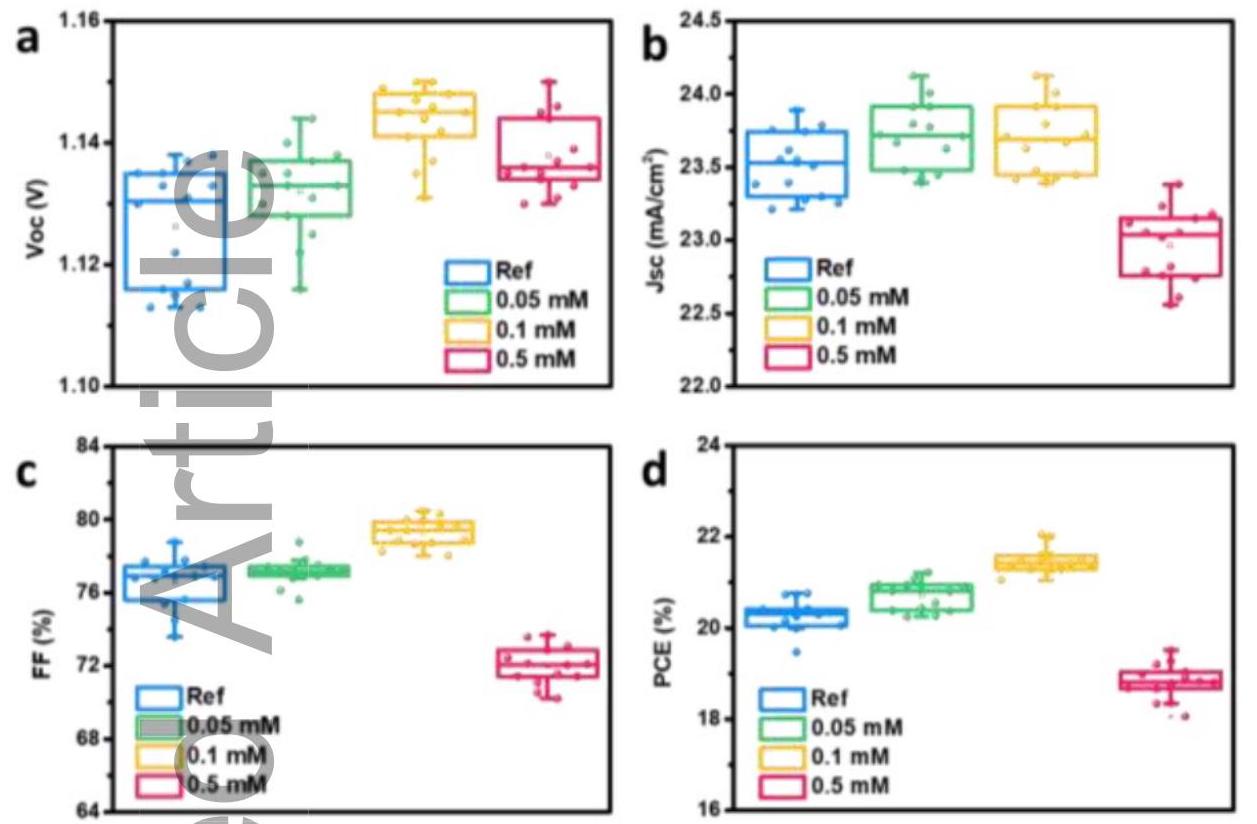
Figure 3. a) The open-circuit voltage (Voc); b) The short-circuit current (Jsc); c) The fill factor (FF); d) The power conversion efficiency (PCE) of perovskite solar cells which fabricated on $0,{0.05}\mathrm{{mM}},{0.1}\mathrm{{mM}}$ , ${0.5}\mathrm{{mM}}{\mathrm{B}}_{2}{\mathrm{{Cat}}}_{2}$ treated ${\mathrm{{SnO}}}_{2}$ films, respectively. Each condition contains 14 devices.
Table 1. Photovoltaic parameters of the PSCs which fabricated on $0,{0.05}\mathrm{{mM}},{0.1}\mathrm{{mM}},{0.5}\mathrm{{mM}}{\mathrm{B}}_{2}{\mathrm{{Cat}}}_{2}$ treated ${\mathrm{{SnO}}}_{2}$ films, respectively.
| Sample | Voc (V) | Jsc $\left( {\mathrm{{mA}}/{\mathrm{{cm}}}^{2}}\right)$ | FF (%) | PCE (%) |
| Ref | 1.126±0.009 | 23.52±0.21 | 76.60±1.33 | 20.29±0.33 |
| 0.05 mM | 1.132±0.007 | 23.71±0.22 | 77.13±0.70 | 20.70±0.31 |
| 0.1 mM | 1.144±0.006 | 23.69±0.23 | 79.29±0.72 | 21.48±0.26 |
| 0.5 mM | 1.138±0.006 | 22.96±0.24 | 72.02±1.01 | ${18.82} \pm {0.38}$ |
To examine the impact of interface, we fabricate n-i-p planar PSCs using SO and BSO films as the ETL, by changing the concentration of ${\mathrm{B}}_{2}{\mathrm{{Cat}}}_{2}$ from ${0.05}\mathrm{{mM}}$ to ${0.5}\mathrm{{mM}}$ , respectively. The device structure is shown in Figure 1a. As summarized in Table 1 and shown in Figure 3, the reference cells (SO based PSCs) give rise to an average PCE of 20.29%, while ${0.1}\mathrm{{mM}}{\mathrm{B}}_{2}{\mathrm{{Cat}}}_{2}$ based cells exhibit the highest average PCE of 21.48%. It can be found that both Voc and FF have significant improvement while increasing the concentration of ${\mathrm{B}}_{2}{\mathrm{{Cat}}}_{2}$ up to ${0.1}\mathrm{{mM}}$ . This indicates the less energy loss and more efficient electron extraction from perovskite to ETL, probably due to the well matched energy level between BSO and perovskite interface. The enhanced charge extraction also brings to the slight increase of short-circuit current (Jsc). When the concentration of ${\mathrm{B}}_{2}{\mathrm{{Cat}}}_{2}$ increases up to ${0.5}\mathrm{{mM}}$ , Jsc and FF of corresponding PSCs drops below that of the reference. We speculate that such a concentration will induce an insulating ${\mathrm{B}}_{2}{\mathrm{{Cat}}}_{2}$ layer between ${\mathrm{{SnO}}}_{2}$ and perovskite, whose thickness is probably beyond the limitation of electron tunnelling. As a result, the PSC devices using ${0.1}\mathrm{{mM}}{\mathrm{B}}_{2}{\mathrm{{Cat}}}_{2}$ treated ${\mathrm{{SnO}}}_{2}$ exhibit the best photovoltaic performance among all the devices. the Voc and FF of devices are significantly improved by ${\mathrm{B}}_{2}{\mathrm{{Cat}}}_{2}$ treatment. Moreover, both SO and BSO based PSCs show negligible J-V hysteresis (Figure S6, Supporting Information), meaning that the introduction of ${\mathrm{B}}_{2}{\mathrm{{Cat}}}_{2}$ brings no extra defects at the interface. In addition, a stabilized efficiency of 21.11% is achieved by holding the voltage at maximum power point for BSO based device, as shown in Figure 4b, while the SO based device only exhibits the stabilized PCE of 20.43% (Figure S7, Supporting Information). Further, we conducted the EQE measurements on the reference (SO) and diboron treated (BSO) devices (Figure S8, Supporting Information). The integrated current values calculated by the EQE spectra for SO and BSO PSCs are 23.12 and ${23.46}\mathrm{\;{mA}}/{\mathrm{{cm}}}^{2}$ , respectively, which close to the J-V measurements. It is apparent that the BSO based device shows significantly higher EQE due to the faster carrier extraction and transportation, resulting less current loss. This further helps to explain the enhancement of device parameters by using diboron treatment.
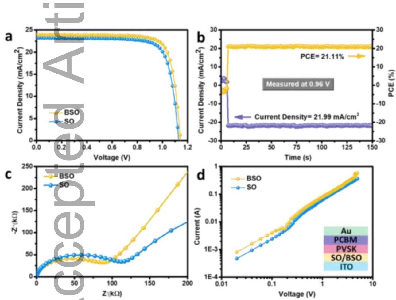
Figure 4. a) J-V curves with reverse $\left( {{1.2}\mathrm{\;V}}\right.$ to $- {0.2}\mathrm{\;V})$ scan of the champion SO and BSO based PSC devices. The scan rate is ${100}\mathrm{{mV}}/\mathrm{s}$ . b) Stabilized PCE at the maximum power point (bias voltage is ${0.96}\mathrm{\;V}$ ) of BSO based PSC device. c) EIS measurements of SO and BSO based PSCs. d) The dark current-voltage characteristics of devices with ITO/SO or BSO/perovskite/PCBM/Au configuration.
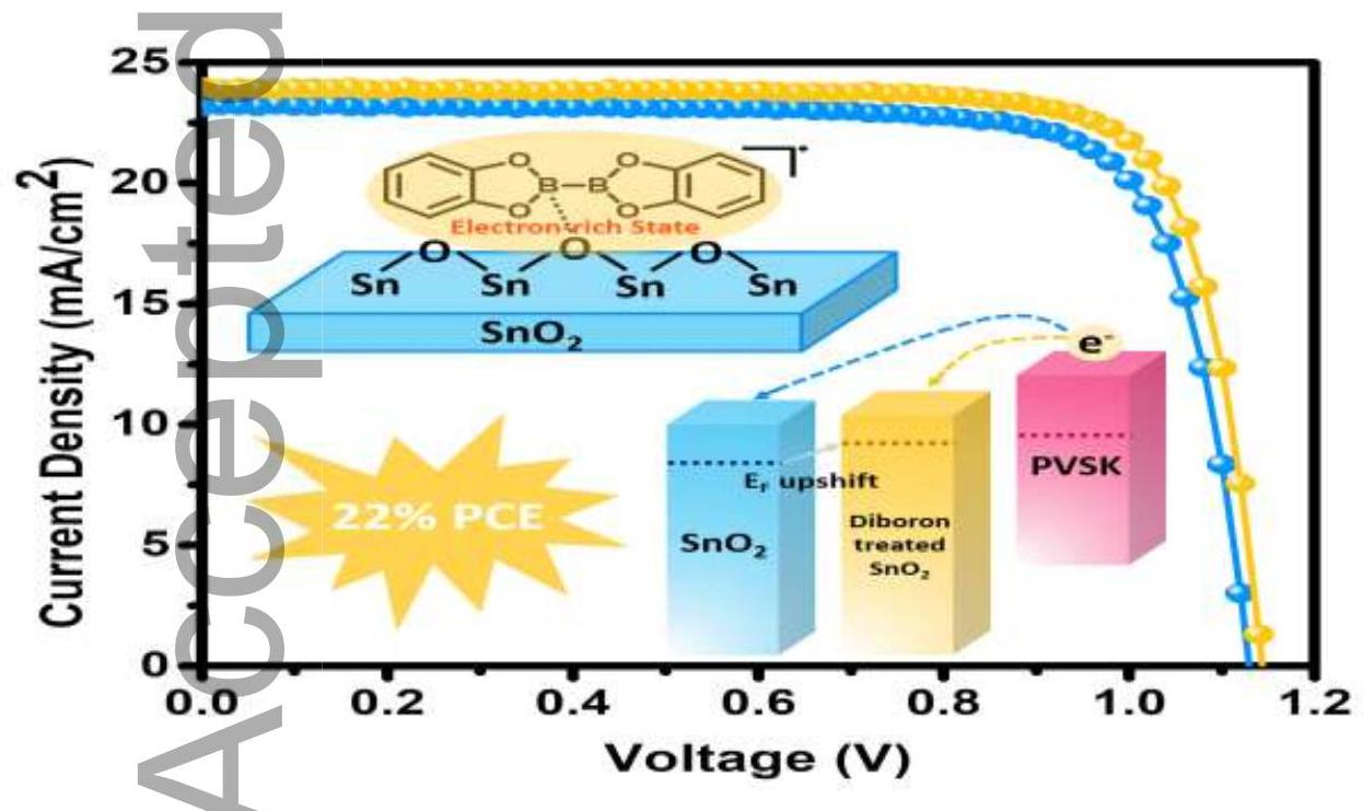
The best BSO based PSC device exhibits a Voc of 1.148 V, Jsc of 23.70 mA/cm ${}^{2}$ , FF of 80.98%, and a PCE of 22.04%. In comparison, the best reference (SO based sample) cgives rise to a Voc of ${1.134}\mathrm{\;V}$ , Jsc of ${23.45}\mathrm{\;{mA}}/{\mathrm{{cm}}}^{2}$ , fill factor (FF) of 77.86%, and a PCE of 20.71%. Figure 4a shows their current density-voltage (J-V) curves, which also indicates that
To further examine the effects of BSO on the carrier dynamics in the perovskite devices, we conducted Nyquist plots of the PSCs which tested in dark with applied bias (Figure 4c). From the two separate arcs we could derive the recombination resistance $\left( {R}_{rec}\right)$ at low-frequency (high resistance) and the contact resistance $\left( {R}_{co}\right)$ at high-frequency (low resistance) ${}^{\left\lbrack {24}\right\rbrack }$ . Obviously, BSO based device has smaller value of ${\mathrm{R}}_{\mathrm{{co}}}$ and higher value of ${\mathrm{R}}_{\mathrm{{rec}}}$ than the SO based cell. The smaller ${\mathrm{R}}_{\mathrm{{co}}}$ means the better electron extraction within the device, confirming the above results, while the larger ${\mathrm{R}}_{\mathrm{{rec}}}$ means that it can effectively suppress the charge recombination to improve the device performance.
To gain the insight into the electron mobility of PSCs, we then fabricated perovskite devices by using the structure: ITO/SO or BSO/perovskite/PCBM/Au, and characterized the evolution of the space-charge-limited current (SCLC) with different biases (Figure 4d). At low bias voltage, carriers from the perovskite films contribute the current, which lead to a linear relationship of I-V curve named “ohmic region”. When the bias voltage increases, injected carriers start to fill the trap states and finally reach the trap-filled limit (TFL), corresponding voltage named " ${\mathrm{V}}_{\mathrm{{TFL}}}$ “. Then with the bias voltage further increases, the current shows a linear relationship with the square of the voltage (I $\propto {\mathrm{V}}^{2}$ ) named “child region”. We thus obtain the carrier mobility from the Mott-Gurney law ${}^{\left\lbrack {25}\right\rbrack } : {J}_{D} = \frac{{9\varepsilon }{\varepsilon }_{0}\mu {V}^{2}}{8{L}^{3}}$ , where the $\varepsilon ,{\varepsilon }_{0}$ and L are the relative dielectric constant, the vacuum permittivity and the thickness of perovskite film, respectively. The electron mobility $\left( {\mu }_{\mathrm{e}}\right)$ of SO and BSO based devices are calculated to be ${0.106}{\mathrm{\;{cm}}}^{2}{\mathrm{\;V}}^{-1}{\mathrm{\;S}}^{-1}$ and ${0.071}{\mathrm{\;{cm}}}^{2}{\mathrm{\;V}}^{-1}{\mathrm{\;S}}^{-1}$ , respectively. The enhancement of electron mobility improves the resulting optoelectronic properties of the PSCs. This is also consistent with reduced PL spectral response and shorter lifetime by TRPL measurement (Figure 2g-h). To clarify whether diboron has passivation effects on the surface states of ${\mathrm{{SnO}}}_{2}$ , we calculate the carrier mobility (which can be influenced by defects scattering) of ETL by using SCLC measurements on the electron-only devices (Figure S9, Supporting Information). We estimate the carrier mobility to be ${1.15} \times {10}^{-3}$ and ${1.21} \times {10}^{-3}{\mathrm{\;{cm}}}^{2}{\mathrm{\;V}}^{-1}{\mathrm{\;S}}^{-1}$ for the SO and BSO devices, respectively. The similar values of carrier mobility among these devices indicate that diboron has no significant passivation effects on the surface states of ${\mathrm{{SnO}}}_{2}$ . Thus the suppressed charge recombination (higher value of ${\mathrm{R}}_{\text{ rec }}$ in BSO based device, Figure 4c) mainly attribute to the better electron extraction and transportation along perovskite $/{\mathrm{{SnO}}}_{2}$ interface.
Finally, we investigated the operational stability of unencapsulated SO and BSO devices under maximum power point (MPP) conditions with a continuous one sun irradiation (LED source) in nitrogen atmosphere (Figure S10, Supporting Information). BSO based device keeps 95% of its initial PCE, while the reference cell drops below 90% after 100 hours. This further confirms the interface treatment by diboron leads to an improvement in the long-term stability of PSCs. We attribute this to the more efficient carrier extraction during operational conditions in BSO based device, thus reducing carrier recombination and further ion migration.
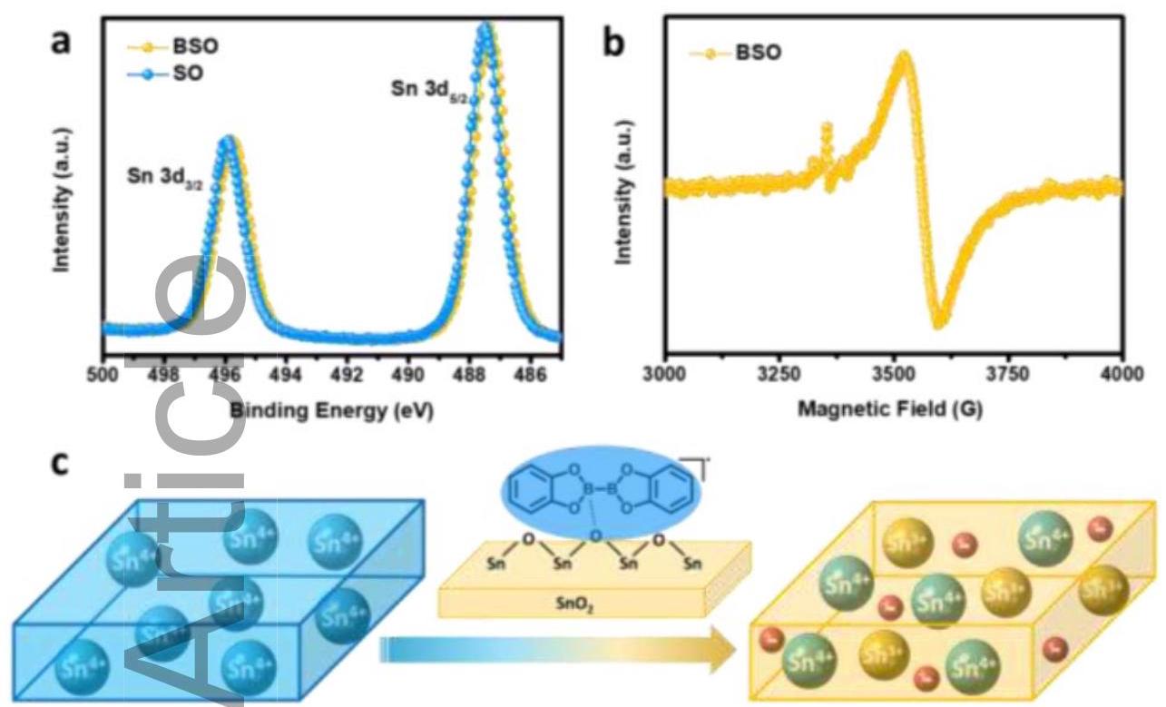
Figure 5. a) The X-ray photoelectron spectroscopy (XPS) spectra of SO and BSO film. b) The electron paramagnetic resonance (EPR) spectra of BSO film. c) The proposed mechanism diagram of ${\mathrm{B}}_{2}{\mathrm{{Cat}}}_{2}$ treated ${\mathrm{{SnO}}}_{2}$ , which contains some ${\mathrm{{Sn}}}^{3 + }$ species as electron donors.
To clearly identify the mechanism of the more n-type nature of ${\mathrm{B}}_{2}{\mathrm{{Cat}}}_{2}$ treated ${\mathrm{{SnO}}}_{2}$ films, we further conduct the X-ray photoelectron spectroscopy (XPS) measurements of SO and BSO films. The $\mathrm{{Sn}}3\mathrm{\;d}$ core-level spectrum of ${\mathrm{{SnO}}}_{2}$ nanoparticles is shown in Figure 5a, and the two peaks correspond to Sn $3{\mathrm{\;d}}_{5/2}$ and Sn $3{\mathrm{\;d}}_{3/2}$ , respectively. For SO film the peaks of Sn $3{\mathrm{\;d}}_{5/2}$ and $\mathrm{{Sn}}3{\mathrm{\;d}}_{3/2}$ are located at487.55and ${495.95}\mathrm{{eV}}$ , while this values of BSO film are 487.34 and ${495.76}\mathrm{{eV}}$ , respectively. It can be noted that the binding energy of $\mathrm{{Sn}}3\mathrm{\;d}$ core-level exhibits a slight shift toward to lower values for BSO films, indicating that the valence state of Sn is likely to be reduced by ${\mathrm{B}}_{2}{\mathrm{{Cat}}}_{2}$ . To further confirm the existence of low valence state of Sn in BSO films, electron paramagnetic resonance (EPR) measurement is conducted, wherein ${\mathrm{{Sn}}}^{3 + }$ with $5{\mathrm{\;s}}^{1}$ electron structure is electron paramagnetic. As shown in Figure 5b, the strong absorption signal of ${\mathrm{{Sn}}}^{3 + }$ is detected in the BSO film ${}^{\left\lbrack {26}\right\rbrack }$ , indicating that ${\mathrm{B}}_{2}{\mathrm{{Cat}}}_{2}$ treatment surely induces some ${\mathrm{{Sn}}}^{3 + }$ species in the ${\mathrm{{SnO}}}_{2}$ film, which can serve as electron donors (Figure 5c). According to the equation which determines the space depletion width (W): $= \sqrt{\frac{{2\varepsilon }{\varepsilon }_{0}\left( {\mathrm{E} - \mathrm{{Ef}}}\right) }{eN}}$ , where $\mathrm{N},\varepsilon {\varepsilon }_{0}$ are the concentration of electron donors, relative dielectric constant, vacuum permittivity, respectively ${}^{\left\lbrack {27}\right\rbrack }$ . The higher donor concentration of BSO film is prone to induce a narrow depletion width, which leads to an enhanced carrier tunnelling probability from perovskite to ETL. These improvements are all beneficial to the carrier extraction and transportation in the entire PSC devices.
In consideration of the chemical properties of diboron, previous study showed that diboron molecules can function as single reducing agents when they are bonded with Lewis basic oxygen atom ${}^{\left\lbrack {28}\right\rbrack }$ . Thus, we speculate that when the ${\mathrm{{SnO}}}_{2}$ films are treated with diboron, the bridging $\mathrm{O}$ or the adsorbed hydroxyl group on the surface of ${\mathrm{{SnO}}}_{2}$ can coordinate with dirboron, resulting a surface diboron-oxygen Lewis pair, inducing a reducing state of diboron complexes (Figure 5c). The single electron can transfer from diboron complexes to the adjacent $\mathrm{{Sn}}$ site, resulting in the formation of ${\mathrm{{Sn}}}^{3 + } - {\mathrm{O}}^{ - }$ species on the surface of ${\mathrm{{SnO}}}_{2}$ film. The presence of ${\mathrm{{Sn}}}^{3 + } - {\mathrm{O}}^{ - }$ species suggests a possible $\mathrm{n}$ type doping, and a high donor concentration on the ETL. It also well explains the up-shift of the Fermi energy of the BSO, which provides an effective means to tune the band alignment in the interfaces.
3. Conclusion
In summary, we have explored an effective interfacial modifier between ${\mathrm{{SnO}}}_{2}$ and perovskite by using the ${\mathrm{B}}_{2}{\mathrm{{Cat}}}_{2}$ molecule. The higher ${\mathrm{E}}_{\mathrm{F}}$ on the surface of ${\mathrm{{SnO}}}_{2}$ (meaning a more n-type property) is obtained based on the ${\mathrm{B}}_{2}{\mathrm{{Cat}}}_{2}$ treatment, which close to the ${\mathrm{E}}_{\mathrm{F}}$ of perovskite, resulting a better energy alignment at ETL/perovskite interface and a higher PCE of 22.04% with negligible hysteresis in planar n-i-p perovskite solar cells. We attribute the improvement in optoelectronic properties to the more efficient carrier extraction and suppressed charge recombination at the ${\mathrm{{SnO}}}_{2}$ /perovskite interface. Moreover, we use XPS and EPR measurements to demonstrate that the ${\mathrm{B}}_{2}{\mathrm{{Cat}}}_{2}$ treated ${\mathrm{{SnO}}}_{2}$ induce some ${\mathrm{{Sn}}}^{3 + }$ species on the surface, which enable a more n-type nature at the ETL/perovskite interface. Considering the chemical properties of ${\mathrm{B}}_{2}{\mathrm{{Cat}}}_{2}$ , we speculate that the formation of surface diboron-oxygen Lewis pair enables a reducing state of diboron complexes, which induce spontaneous electron injection from ${\mathrm{O}}^{2 - }$ to adjacent ${\mathrm{{Sn}}}^{4 + }$ leading to an extremely stable surface ${\mathrm{{Sn}}}^{3 + } - {\mathrm{O}}^{- - }$ complex. This provides an effective chemical approach to tuning the energy level alignment at the ETL/perovskite interfaces.
Acknowledgements
N.L. and X.N. contributed equally to this work. This work is supported by National Natural Science Foundation of China (51722201) (51672008) (91733301), National Key Research and Development Program of China Grant No. 2017YFA0206701, Natural Science Foundation of Beijing, China (Grant No. 4182026), Young Talent Thousand Program. National Key Research and Development Program of China Grant No. 2016YFB0700700, National Natural Science Foundation of China (51673025), Beijing Municipal Science and Technology Project No. Z181100005118002.
N.L. and X.N. contributed equally to this work. This work is supported by National Natural Science Foundation of China (51722201) (51672008) (91733301), National Key Research and Development Program of China Grant No. 2017YFA0206701, Natural Science Foundation of Beijing, China (Grant No. 4182026), Young Talent Thousand Program. National Key Research and Development Program of China Grant No. 2016YFB0700700, National Natural Science Foundation of China (51673025), Beijing Municipal Science and Technology Project No. Z181100005118002.
Conflict of Interest
The authors declare no conflict of interest.
Keywords
Diboron, perovskites, solar cells, interface engineering, high efficiency
References
[1] a) M. A. Green, A. H. Baillie, H. J. Snaith, Nat. Photonics 2014, 8, 506; b) M. Liu, M. B. Johnston, H. J. Snaith, Nature 2013, 501, 395; c) N. J. Jeon, J. H. Noh, W. S. Yang, Y. C. Kim, S. Ryu, J. Seo, S. I. Seok, Nature 2015, 517, 476; d) Q. Lin, A. Armin, R. C. R. Nagiri, P. L. Burn, P. Meredith, Nat. Photonics 2015, 9, 106.
[2] a) Z. Xiao, R. A. Kerner, L. Zhao, N. L. Tran, K. M. Lee, T. W. Koh, G. D. Scholes, B. P. Rand Nat. Photonics 2017, 11, 108; b) K. Lin, J. Xing, L. N. Quan, F. P. G. Arquer, X. Gong, J. Lu, L. Xie, W. Zhao, D. Zhang, C. Yan, W. Li, X. Liu, Y. Lu, J. Kirman, E. H. Sargent, Q. Xiong, Z. Wei, Nature 2018, 562, 245; c) L. Zhao, K. M. Lee, K. Roh, S. U. Z. Khan, B. P. Rand, Adv. Mater. 2019, 31, 1805836.
[3] a) Y. Fang, J. Huang, Adv. Mater. 2015, 27, 2804; b) H. Sun, W. Tian, F. Cao, J. Xiong, L. Li Adv. Mater. 2018, 30, 1706986. c) L. Dou, Y. Yang, J. You, Z. Hong, W. H. Chang, G. Li, Y. Yang Nat. Commun. 2014, 5, 5404
[4] A. Kojima, K. Teshima, Y. Shirai, T. Miyasaka J. Am. Chem. Soc. 2009, 131, 6050.
[5] C. Wehrenfennig, G. E. Eperon, M. B. Johnston, H. J. Snaith, L. M. Herz, Adv. Mater. 2014, 26, 1584.
[6] H. J. Snaith, J. Phys. Chem. Lett. 2013, 4, 3623.
[7] a) M. M. Lee, J. Teuscher, T. Miyasaka, T. N. Murakami, H. J. Snaith, Science 2012, 338, 643; b) H. Zhou, Q. Chen, G. Li, S. Luo, T. Song, H. S. Duan, Z. Hong, J. You, Y. Liu, Y. Yang, Science 2014, 345, 542; c) Q. Jiang, Z. Chu, P. Wang, X. Yang, H. Liu, Y. Wang, Z. Yin, J. Wu, X. Zhang, J. You, Adv. Mater. 2017, 29, 1703852. d) Best Research-Cell Efficiency Chart. 2019, https://www.nrel.gov/pv/cell-efficiency.html.
[8] a) W. S. Yang, J. H. Noh, N. J. Jeon, Y. C. Kim, S. Ryu, J. Seo, S. I. Seok, Science 2015, 348, 1234; b) Q. Chen, H. Zhou, Z. Hong, S. Luo, H. S. Duan, H. H. Wang, Y. Liu, G. Li, Y. Yang J. Am. Chem. Soc. 2014, 136, 622.
[9] a) N. Li, S. Tao, Y. Chen, X. Niu, C. K. Onwudinanti, C. Hu, Z. Qiu, Z. Xu, G. Zheng, L. Wang, Y. Zhang, L. Li, H. Liu, Y. Lun, J. Hong, X. Wang, Y. Liu, H. Xie, Y. Gao, Y. Bai, S. Yang, G. Brocks, Q. Chen, H. Zhou, Nat. Energy 2019, 4, 408. b) W. S. Yang, B. W. Park, E. H. Jung, N. J. Jeon, Y. C. Kim, D. U. Lee, S. S. Shin, J. Seo, E. K. Kim, J. H. Noh, S. I. Seok, Science 2017, 356, 1376.
This article is protected by copyright. All rights reserved
[10] H. J. Snaith, C. Ducati, Nano Lett. 2010, 10, 1259.
[11] L. Yang, B. Xu, D. Bi, H. Tian, G. Boschloo, L. Sun, A. Hagfeldt, E. M. J. Johansson, J. Am. Chem. Soc. 2013, 135, 7378.
[12] J. Xu, A. Buin, A. H. Ip, W. Li, O. Voznyy, R. Comin, M. Yuan, S. Jeon, Z. Ning, J. J. McDowell, P. Kanjanaboos, J. P. Sun, X. Lan, L. N. Quan, D. H. Kim, I. G. Hill, P. Maksymovych, E. H. Sargent, Nat. Commun. 2015, 6, 7081.
[13] a) J. M. Ball, A. Petrozza, Nat. Energy 2016, 1, 16149. b) T. S. Sherkar, C. Momblona, L. G. Escrig, J. Ávila, M. Sessolo, H. J. Bolink, L. J. A. Koster, ACS Energy Lett. 2017, 2, 1214.
[14] a) J. M. Azpiroz, E. Mosconi, J. Bisquert, F. D. Angelis, Energy Environ. Sci. 2015, 8, 2118. b) N. Ahn, K. Kwak, M. S. Jang, H. Yoon, B. Y. Lee, J. K. Lee, P. V. Pikhitsa, J. Byun, M. Choi, Nat. Commun. 2016, 7, 13422.
[15] T. H. Han, M. R. Choi, S. H. Woo, S. Y. Min, C. L. Lee, T. W. Lee, Adv. Mater. 2012, 24, 1487.
[16] Q. Jiang, Y. Zhao, X. Zhang, X. Yang, Y. Chen, Z. Chu, Q. Ye, X. Li, Z. Yin, J. You, Nat. Photonic 2019, https://doi.org/10.1038/s41566-019-0398-2.
[17] W. Okada, T. Suga, K. Oyaizu, H. Segawa, H. Nishide, ACS Appl. Energy Mater. 2019, 2, 2848.
[18] D. Yang, R. Yang, K. Wang, C. Wu, X. Zhu, J. Feng, X. Ren, G. Fang, S. Priya, S. Liu, Nat. Commun. 2018, 9, 3239.
[19] K. T. Cho, S. Paek, G. Grancini, C. R. Carmona, P. Gao, Y. Lee, M. K. Nazeeruddin, Energy Environ. Sci. 2017, 10, 621.
[20] Q. Jiang, L. Zhang, H. Wang, X. Yang, J. Meng, H. Liu, Z. Yin, J. Wu, X. Zhang, J. You, Nat. Energy 2016, 2, 16177.
[21] J. Shi, X. Xu, D. Li, Q. Meng, Small 2015, 11, 2472.
[22] C. Bi, Q. Wang, Y. Shao, Y. Yuan, Z. Xiao, J. Huang, Nat. Commun. 2015, 6, 7747.
[23] Y. Q. Zhou, B. S. Wu, G. H. Lin, Z. Xing, S. H. Li, L. L. Deng, D. C. Chen, D. Q. Yun, S. Y. Xie, Nat. Commun. 2018, 8, 1800399.
[24] X. Niu, N. Li, C. Zhu, L. Liu, Y. Zhao, Y. Ge, Y. Chen, Z. Xu, Y. Lu, M. Sui, Y. Li, A. Tarasov, E. A. Goodilin, H. Zhou, Q. Chen, J. Mater. Chem. A, 2019, 7, 7338.
[25] Y. Huang, L. Li, Z. Liu, H. Jiao, Y. He, X. Wang, R. Zhu, D. Wang, J. Sun, Q. Chen, H. This article is protected by copyright. All rights reserved
Zhou, J. Mater. Chem. A 2017, 5, 8537.
[26] A. T. Brant, L. E. Halliburton, N. C. Giles, S. A. Basun, A. A. Grabar, D. R. Evans, J. Phys.: Condens. Matter 2013, 25, 205501.
[27] Z. Liu, Q. Chen, Z. Hong, H. Zhou, X. Xu, N. D. Marco, P. Sun, Z. Zhao, Y. B. Cheng, Y. Yang, ACS Appl. Mater. Interfaces 2016, 8, 11076.
[28] a) F. Mo, Y. Jiang, D. Qiu, Y. Zhang, J. Wang, Angew Chem Int Edit 2010, 49, 1846. b) G. Wang, H. Zhang, J. Zhao, W. Li, J. Cao, C. Zhu, S. Li, Angew Chem Int Edit 2016, 55, 5985. c) F. Mo, D. Qiu, Y. Zhang, J. Wang, Accounts Chem Res, 2018, 51, 496.
IIIV Pordenov
TOC Text
Diboron treated ${\mathrm{{SnO}}}_{2}$ possesses some ${\mathrm{{Sn}}}^{3 + }$ species, which serve as electron donors with more n-type nature, resulting the higher Femi level on the surface of ${\mathrm{{SnO}}}_{2}$ , promoting electron extraction and reducing carrier recombination in ETL/perovskite interface. A power conversion efficiency of 22.04 % is obtained in an n-i-p structure perovskite solar cell.