Diboron-Assisted Interfacial Defect Control Strategy for Highly Efficient Planar Perovskite Solar Cells
中文 / Bilingual · English version
Yongguang Tu, Xiaoyu Yang, Rui Su, Deying Luo, Yang Cao, Lichen Zhao, Tanghao Liu, Wenqiang Yang, Yifei Zhang, Zhaojian Xu, Quanzhen Liu, Jihuai Wu, Qihuang Gong, Fanyang Mo, and Rui Zhu*
Metal halide perovskite films are endowed with the nature of ions and polycrystallinity. Formamidinium iodide (FAI)-based perovskite films, which include large cations (FA) incorporated into the crystal lattice, are most likely to induce local defects due to the presence of the unreacted FAI species. Here, a diboron-assisted strategy is demonstrated to control the defects induced by the unreacted FAI both inside the grain boundaries and at the surface regions. The diboron compound $\left( {{\mathrm{C}}_{12}{\mathrm{H}}_{10}{\mathrm{\;B}}_{2}{\mathrm{O}}_{4}}\right)$ can selectively react with unreacted FAI, leading to reduced defect densities. Nonradiative recombination between a perovskite film and a hole-extraction layer is mitigated considerably after the introduction of the proposed approach and charge-carrier extraction is improved as well. A champion power conversion efficiency of 21.11% is therefore obtained with a stabilized power output of 20.83% at the maximum power point for planar perovskite solar cells. The optimized device also delivers negligible hysteresis effect under various scanning conditions. This approach paves a new way for mitigating defects and improving device performance.
Perovskite solar cells (PSCs) have inspired burgeoning interests for making skyrocketing revolution in new type photovoltaic field, ${}^{\left\lbrack 1 - 9\right\rbrack }$ because of their excellent photovoltaic and optoelectronic properties. ${}^{\left\lbrack {10}\right\rbrack }$ Most of the reported perovskites are lead (Pb)-based materials in the form of ${\mathrm{{APbX}}}_{3}$ , where $\mathrm{A}$ is organic cation ${\mathrm{{CH}}}_{3}{\mathrm{{NH}}}_{3}{}^{ + }$ (MA) and $\mathrm{X}$ is halide anion iodide (I ${}^{ - }$ ). Both the organic cation and halide anion can be partially substituted. For instance, ${\mathrm{{CH}}}_{3}{\mathrm{{NH}}}_{3}{}^{ + }$ (MA) cation has been replaced with ${\mathrm{{NH}}}_{2}{\mathrm{{CHNH}}}_{2}{}^{ + }{\left( \mathrm{{FA}}\right) }^{\left\lbrack {11},{12}\right\rbrack }$ and/or cesium ion $\left( {\mathrm{{Cs}}}^{ + }\right) ,{}^{\left\lbrack {13}\right\rbrack }$ also iodide $\left( {\mathrm{I}}^{ - }\right)$ can be exchanged by bromide $\left( {\mathrm{{Br}}}^{ - }\right) ,{}^{\left\lbrack {14}\right\rbrack }$ to deliver mixed-cation lead mixed-halide perovskite. The devices with the optimized perovskite have been proven to remarkable stability and impressive power conversion efficiency (PCE). ${}^{\left\lbrack {13},{15},{16}\right\rbrack }$
The precursor solution of mixed-cation lead mixed-halide perovskite is featured with colloidal chemistry, where it has soft coordination complex of ${\left\lbrack {\mathrm{{PbI}}}_{6}\right\rbrack }^{4 - }$ cages with organic cations. ${}^{\left\lbrack {17},{18}\right\rbrack }$ Coupled with complex crystallization process, the resulting perovskite films could induce inhomogeneous composition distribution and local unreacted species in bulk materials and/or at the surface. ${}^{\left\lbrack {19},{20}\right\rbrack }$ Typically, the unreacted ${\mathrm{{PbI}}}_{2}$ has been found to be present within the perovskite film, ${}^{\left\lbrack {21}\right\rbrack }$ which has positive impact on improving device performance through passivation roles. ${}^{\left\lbrack {22} - {26}\right\rbrack }$
For the organic-halide species, evidences suggest that there were some unre-acted formamidinium iodide (FAI) species existing throughout the perovskite film, ${}^{\left\lbrack {19},{21}\right\rbrack }$ exhibiting a FAI-rich region close to the surface of the perovskite film. Such FAI species normally cause the reduction in device performance owing to increase in ionic defects. Moreover, Snaith et al. ${}^{\left\lbrack {27}\right\rbrack }$ proposed unreacted ions (iodide or MA) throughout the film may accelerate the hysteresis effect by ion migrations. Similarly, Jacobsson et al.[21] found that the accumulation of unreacted organic-halide species in the grain boundaries would hinder the charge-carrier transportation and extraction, and even acted as nonradiative recombination centers. ${}^{\left\lbrack {19},{28}\right\rbrack }$ The elimination of undesirable organic-halide species, however, remains open questions in the perovskite solar cells. As a result, it is warranted to develop a facile method to reduce defects and/or nonradiative recombination centers by eliminating the unreacted organic-halide species, aiming to improve charge-carrier extraction and device efficiency.
Dr. Y. Tu, X. Yang, R. Su, D. Luo, L. Zhao, Dr. T. Liu, W. Yang, Y. Zhang, Z. Xu, Prof. Q. Gong, Prof. R. Zhu
State Key Laboratory for Artificial Microstructure
and Mesoscopic Physics
Department of Physics
Peking University
Beijing 100871, China
D. Luo, Prof. Q. Gong, Prof. R. Zhu
Collaborative Innovation Center of Quantum Matter
Beijing 100871, China
Dr. Y. Cao, Prof. F. Mo
Department of Energy and Resources Engineering
College of Engineering
Peking University
Beijing 100871, China
Q. Liu, Prof. J. Wu
Engineering Research Center of Environment-Friendly Functional
Materials for Ministry of Education
Institute of Materials Physical Chemistry
College of Material Science and Engineering
Huaqiao University
Xiamen, Fujian 361021, China
Prof. Q. Gong, Prof. R. Zhu
Collaborative Innovation Center of Extreme Optics
Shanxi University
Taiyuan, Shanxi 030006, China
DOI: 10.1002/adma.201805085
DOI: 10.1002/adma.201805085
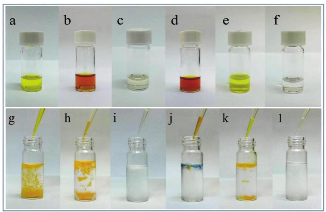
Figure 1. Photographs of different solutions. a) Reference perovskite precursor solution. b) Perovskite precursor solution with addition 3 wt% ${\mathrm{B}}_{2}{\mathrm{{Cat}}}_{2}$ . c) FAI solution. d) FAI solution with ${\mathrm{B}}_{2}{\mathrm{{Cat}}}_{2}$ . e) ${\mathrm{{PbI}}}_{2}$ solution with ${\mathrm{B}}_{2}{\mathrm{{Cat}}}_{2}$ . f) ${\mathrm{B}}_{2}{\mathrm{{Cat}}}_{2}$ solution. Chromogenic reaction with starch aqueous solution. g) Reference perovskite precursor solution. h) Perovskite precursor solution with additional 3 wt% ${\mathrm{B}}_{2}{\mathrm{{Cat}}}_{2}$ . i) FAI solution. j) FAI solution with ${\mathrm{B}}_{2}{\mathrm{{Cat}}}_{2}$ . k) ${\mathrm{{PbI}}}_{2}$ solution with ${\mathrm{B}}_{2}{\mathrm{{Cat}}}_{2}$ . I) ${\mathrm{B}}_{2}{\mathrm{{Cat}}}_{2}$ solution.
Herein, we demonstrate a diboron-assisted strategy to decompose the unreacted organic-halide species at the surface by coating ${\mathrm{B}}_{2}{\mathrm{{Cat}}}_{2}\left( {{\mathrm{C}}_{12}{\mathrm{H}}_{10}{\mathrm{\;B}}_{2}{\mathrm{O}}_{4}}\right)$ on top of the perovskite films. A gaseous medium was produced from chemical reaction between FAI and ${\mathrm{B}}_{2}{\mathrm{{Cat}}}_{2}$ at elevated temperature that led to a “clean” region between the perovskite film and the hole-extraction layer. Meanwhile, the diboron-assisted strategy is expected to suppress the nonradiative recombination losses. Finally, the perovskite solar cells with the regular planar structure exhibited a champion PCE of 21.11% compared to that of the control device (PCE of 19.61%) with a stabilized power output of 20.83%, and negligible hysteresis effect under various scanning condition.
Figure 1 shows the photographs of different solutions, where a series of solutions were prepared to investigate the reaction between ${\mathrm{B}}_{2}{\mathrm{{Cat}}}_{2}$ (the chemical structure was present in Figure S1 in the Supporting Information) and perovskite component materials. To ensure a single variable, the solutions used the same precursors and solvents as reference perovskite precursors. As shown in Figure 1a, the reference perovskite precursor solution in N, N-dimethylformamide (DMF):dimethyl sulfoxide (DMSO) (v/v = 4:1) delivered a yellow color. Specifically, when 3 wt% of ${\mathrm{B}}_{2}{\mathrm{{Cat}}}_{2}$ was added into the perovskite precursor solution, the color turned to slight brown, as shown in Figure 1b. Brown also appeared when same ${\mathrm{B}}_{2}{\mathrm{{Cat}}}_{2}$ was added into the colorless FAI solution, as shown in Figure 1c, d. PbI ${}_{2}$ solution still maintained the initial yellow color after the addition of ${\mathrm{B}}_{2}{\mathrm{{Cat}}}_{2}$ (Figure 1e). In particular, the ${\mathrm{B}}_{2}{\mathrm{{Cat}}}_{2}$ solution was colorless (Figure 1f). Mixed solution of other low content perovskite components (such as ${\mathrm{{PbBr}}}_{2}$ , MABr, and $\mathrm{{CsI}}$ ) with ${\mathrm{B}}_{2}{\mathrm{{Cat}}}_{2}$ was also prepared, as shown in Figure S2 in the Supporting Information. The ${\mathrm{{PbBr}}}_{2}$ solution with ${\mathrm{B}}_{2}{\mathrm{{Cat}}}_{2}$ and the MABr solution with ${\mathrm{B}}_{2}{\mathrm{{Cat}}}_{2}$ both presented the original intrinsic color (Figure S2a-d, Supporting Information). While the CsI solution with ${\mathrm{B}}_{2}{\mathrm{{Cat}}}_{2}$ turned to slight yellow from colorless (Figure S2e, f, Supporting Information). Considering FAI was the main component in perovskite precursor (the molar ratio of FAI: CsI was nearly 20/1), we can speculate that the brown color came mainly from the reaction of FAI and ${\mathrm{B}}_{2}{\mathrm{{Cat}}}_{2}$ .
To further investigate the discoloration feature, chromogenic reaction of the various solutions with starch aqueous solutions was carried out. In Figure 1j, When the FAI-B2 ${\mathrm{{Cat}}}_{2}$ solution was added into starch aqueous solution, blue appeared in colorless solution, which indicated directly the existence of iodine in the brown solution. ${}^{\left\lbrack {29}\right\rbrack }$ In contrast, in Figure 1g, k, for reference perovskite precursor solution and ${\mathrm{{PbI}}}_{2} - {\mathrm{B}}_{2}{\mathrm{{Cat}}}_{2}$ solution, when both solutions added in the starch aqueous solution respectively, it was observed that the precipitation of lead iodide occurred without color change. In Figure 1h, when the slight brown perovskite precursor solution with 3 wt% ${\mathrm{B}}_{2}{\mathrm{{Cat}}}_{2}$ was added, no blue color was observed, which may be attributed to two factors: trace iodine content in the slight brown solution and dominant yellow precipitation of the precursor. In Figure 1i, l, when the colorless FAI and ${\mathrm{B}}_{2}{\mathrm{{Cat}}}_{2}$ solutions dripped separately into the starch aqueous solution, there was still no color change.
We did extreme experiment to investigate the reaction between FAI and ${\mathrm{B}}_{2}{\mathrm{{Cat}}}_{2}$ in two-phase reaction. As reported, the mass loss of FAI starts from $\approx {247}^{ \circ }\mathrm{C}$ by thermogravimetry differential scanning calorimetry analysis, ${}^{\left\lbrack {30}\right\rbrack }$ so FAI is not easily removed by heating at ${100}{}^{ \circ }\mathrm{C}$ (as shown in Figure S3 in the Supporting Information). Figure S4a in the Supporting Information shows the annealed FAI film on the indium tin oxide (ITO) substrate. When ${\mathrm{B}}_{2}{\mathrm{{Cat}}}_{2}/$ isopropyl alcohol (IPA) solution was dripped onto the FAI film (Figure S4b, Supporting Information), the white FAI disappeared gradually with heating (Figure S4c, Supporting Information). At last, the reactants disappeared almost (Figure S4d, Supporting Information). Based on above observation, we conclude that ${\mathrm{B}}_{2}{\mathrm{{Cat}}}_{2}$ could react with FAI and there is almost no residue eventually. To explore the reaction mechanism, we further carried out the proton nuclear magnetic resonance (1H-NMR) spectra of FAI, ${\mathrm{B}}_{2}{\mathrm{{Cat}}}_{2}$ and ${\mathrm{{FAI} - B}}_{2}{\mathrm{{Cat}}}_{2}$ mixture (DMSO- ${d}_{6},{400}\mathrm{{MHz}}$ ), as shown in Figures S5-S7 in the Supporting Information (specific mechanism analysis could be found in the Supporting Information).
Based on above analysis, a schematic diagram delivering the reduction of the unreacted FAI species with ${\mathrm{B}}_{2}{\mathrm{{Cat}}}_{2}$ - assisted strategy is given in Figure 2a. The control film was composed of cesium-containing triple cation perovskite. $5\mathrm{{mg}}{\mathrm{{mL}}}^{-1}{\mathrm{\;B}}_{2}{\mathrm{{Cat}}}_{2}/$ IPA solution was deposited on top of the perovskite film by spin coating, hereafter termed as B-film (see Experimental Section).
To assess the change in compositions to the films with and without ${\mathrm{B}}_{2}{\mathrm{{Cat}}}_{2}$ treatments, X-ray photoelectron spectroscopy (XPS) that is a surface sensitive technique ${}^{\left\lbrack {31},{32}\right\rbrack }$ was performed. The overview spectrum of the prepared perovskite film is present in Figure S9 in the Supporting Information, and the core level peaks obtained were indexed to the elements forming perovskite materials. ${}^{\left\lbrack {19},{28}\right\rbrack }$ High-resolution spectra of Pb 4f, I 4d, and $\mathrm{N}1\mathrm{\;s}$ regions are shown in Figure $2\mathrm{\;b}$ and Figure S10 in the Supporting Information, respectively. By normalizing the spectra with respect to the Pb $4{\mathrm{f}}_{7/2}$ peak, there is a noticeable decrease in I 4d and $\mathrm{N}1\mathrm{\;s}$ of the B-film related to the decomposition of the FAI close to the surface of the perovskite film. For ${\mathrm{{FA}}}_{0.81}{\mathrm{{MA}}}_{0.10}{\mathrm{{Cs}}}_{0.04}{\mathrm{{PbI}}}_{2.55}{\mathrm{{Br}}}_{0.40}$ in our specific experiment, the theoretical I/Pb ratio value based on the bulk stoichiometry is 2.55. The ions stoichiometry ratio in the material was investigated by comparing the integral area of the characteristic peaks. ${}^{\left\lbrack {19},{21},{28}\right\rbrack }$ The I/Pb ratio with standard error was estimated to be ${2.90} \pm {0.0619}$ and ${2.70} \pm {0.0387}$ for the control and B-film, respectively, as shown in Figure S11 in the Supporting Information. (More information about XPS statistical results were listed in Table S1 in the Supporting Information.) This means that the residual FAI species within the B-film is less than that of the control film. ${}^{\left\lbrack {21}\right\rbrack }$
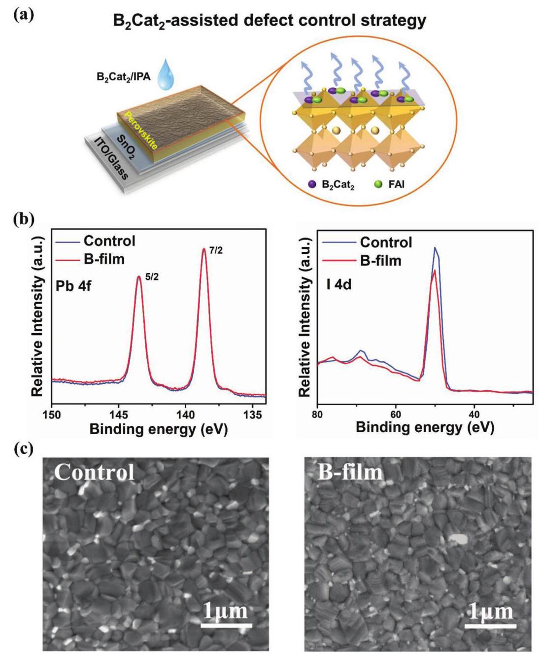
Figure 2. a) Schematic view of the ${\mathrm{B}}_{2}{\mathrm{{Cat}}}_{2}$ -assisted defect control strategy. b) The high-resolution spectra of X-ray photoelectron spectroscopy for Pb 4f and I 4d regions on the surface of the prepared perovskite film. c) SEM images of the control and B-film.
To further demonstrate the influence of the ${\mathrm{B}}_{2}{\mathrm{{Cat}}}_{2}$ treatment on the perovskite film, below we performed a morphological and crystallographic characterization of the prepared films. As shown in Figure 2c, the constitutive grain size of the control and B-film is among ${200} - {300}\mathrm{\;{nm}}$ , indicating that ${\mathrm{B}}_{2}{\mathrm{{Cat}}}_{2}$ did not notably change the morphology and grain size of the perovskite films. The “bright crystals” on the surface was mainly dominated by lead halide complex. ${}^{\left\lbrack {33}\right\rbrack }$ The X-ray diffraction (XRD) results show that there is no notable change in the crystallinity from the XRD patterns after introducing ${\mathrm{B}}_{2}{\mathrm{{Cat}}}_{2}$ treatment (Figure S12, Supporting Information). The peak at ${12.7}^{ \circ }$ could be indexed to the (001) lattice plane of crystallized ${\mathrm{{PbI}}}_{2}{.}^{\left\lbrack {34},{35}\right\rbrack }$ The two main peaks for all perovskite films approximately located at ${14.4}^{ \circ }$ and ${28.8}^{ \circ }$ can be indexed to the (110) and (220) planes.[36]
Figure 3a compares the variation in work function and valence band for the control and B-film. Work function determined from secondary cutoff spectrum shows a slight decrease relative to control film, and amplitude in fluctuations is approaching 120 meV. In addition to work function, the valence band maximum with respect to Fermi level also exhibits a 180 meV decrease, as shown in Figure S13 in the Supporting Information. This result indicates that the energy level moves toward vacuum after introducing ${\mathrm{B}}_{2}{\mathrm{{Cat}}}_{2}$ treatments, and such changes in electronic states at the surface further confirm that the surface of the perovskite B-film was healed. The band gaps of both films extracted from Tauc plots show an identical value of ${1.61}\mathrm{{eV}}$ (Figure S14, Supporting Information), in agreement with changes to the films solely present at the surface. Combined with ultraviolet photoelectron spectroscopy (UPS) and absorption, we built an energy-band diagram going from control to B-film. The upward shift of the valence band maximum position for the B-film might be favorable for photogerenated hole extraction from perovskite films to hole-extraction layers. ${}^{\left\lbrack {37}\right\rbrack }$
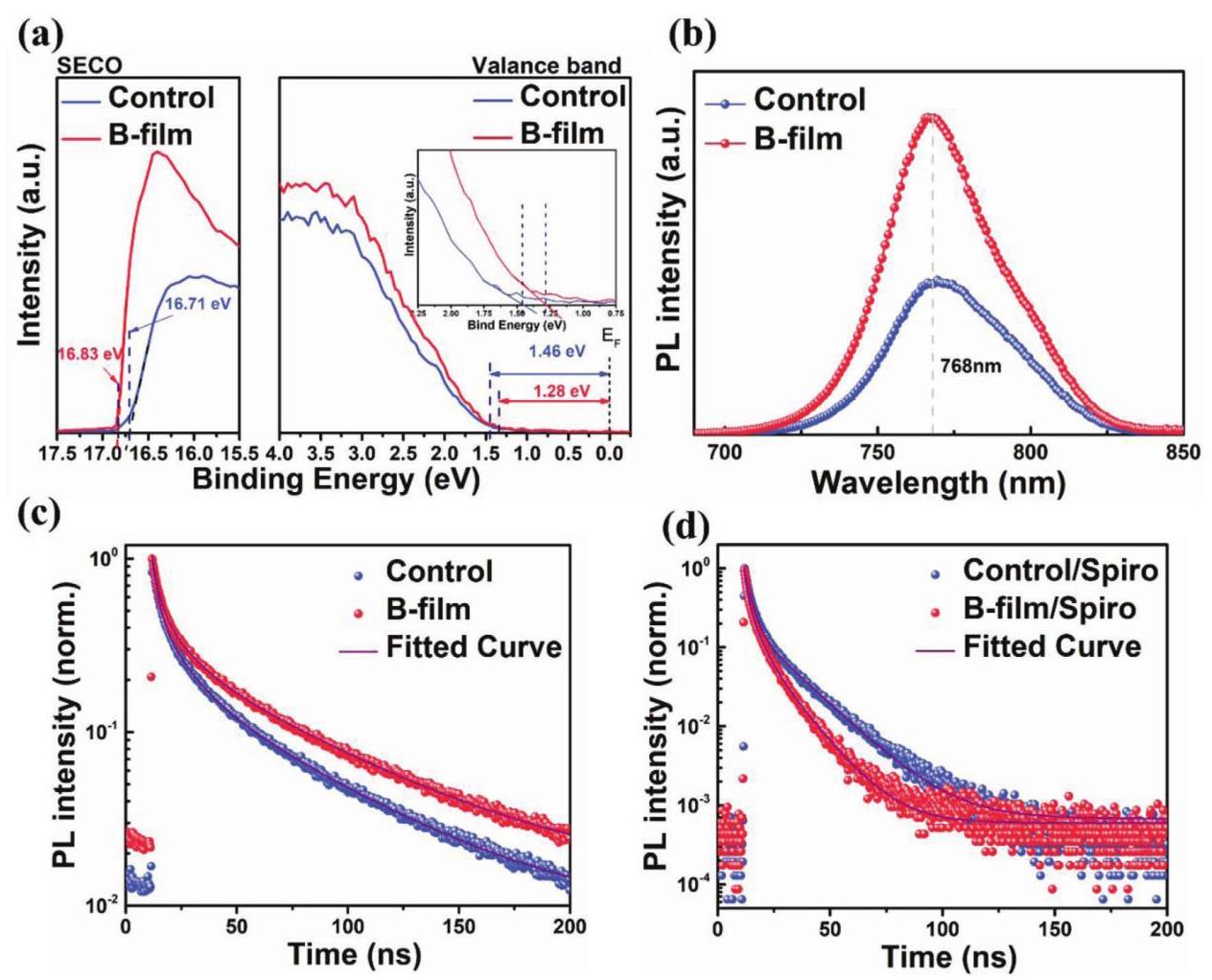
Figure 3. a) UPS spectra of the control and B-film. Left panel: secondary electron cutoff. Right panel: valence band spectrum. b) Steady-state photoluminescence spectra of perovskite films on glass detected at 460 nm excitation wavelength. c) Time-resolved photoluminescence spectra of perovskite films deposited on glass detected at ${768}\mathrm{\;{nm}}$ emission wavelength. d) Time-resolved photoluminescence spectra of the prepared perovskite films detected at 768 nm emission wavelength with the configuration of glass/perovskite/Spiro-OMeTAD.
To gain more insight into charge-carrier dynamics with the change of electronic states, we carried out steady-state photoluminescence (PL) spectroscopy and time-resolved PL (TRPL) intensity decay measurements on series of samples: glass/perovskite and glass/perovskite/hole transporting layer. Figure 3b shows that the B-film exhibited a stronger band emission at ${768}\mathrm{\;{nm}}$ relative to the control film at the same excitation. This confirms that radiative recombination rates from photogenerated charge carriers competitive with nonradiative losses play predominant roles in recombination processes. This is in the right direction to enhance device efficiencies by mitigating nonradiative losses. Figure 3c shows the TRPL decays of the films without hole quenchers, where the curves were fitted with a two-component exponential decay function. The fitted results for the TRPL decays of the B-film delivered a much longer PL decay than that of the control film, attributed to reduced trap-assisted recombination at defect sites. ${}^{\left\lbrack 8,{38}\right\rbrack }$ (More information about TRPL results were given in Figure S15 and Table S2 in the Supporting Information.) In addition, to elucidate the charge-carrier dynamics at the perovskite/Spiro-OMeTAD interface, we further carried out TRPL measurement of the control and B-film with the configuration of glass/perovskite/Spiro-OMeTAD, as shown in Figure 3d (for more information about TRPL results were given in Figure S16 and Table S3 in the Supporting Information.) The B-film had a smaller lifetime versus control film, which indicated that charge injection of the B-film to hole transport layer is more efficient than control film, ${}^{\left\lbrack {39},{40}\right\rbrack }$ in line with the more efficient carrier injection of the perovskite film in Figure 3a.
Figure 4 shows the photovoltaic performances of the perovskite solar cells based on control and B-film. Device structure is shown in Figure 4a. As shown in Figure 4b, the cross-section scanning electron microscopy (SEM) image of B-film device shows a dense and uniform perovskite in the device. A complete comparison of the photocurrent-voltage $\left( {J - V}\right)$ curves of the devices by forward and reverse scans measured under AM 1.5 G (100 mW cm ${}^{-2}$ ) is shown in Figure 4c-e, and the corresponding photovoltaic parameters are listed in Table 1. A PCE of 19.61% was achieved for the control device presenting obvious hysteresis effect, with an open circuit voltage $\left( {V}_{\mathrm{{oc}}}\right)$ of 1.143 V, a short-circuit current density $\left( {J}_{\mathrm{{sc}}}\right)$ of ${22.57}\mathrm{\;{mA}}{\mathrm{\;{cm}}}^{-2}$ , and a fill factor (FF) of 0.76 . For the B-film, device performances with different concentrations $(0,1,3,5$ , and $7\mathrm{{mg}}{\mathrm{{mL}}}^{-1}$ ) of ${\mathrm{B}}_{2}{\mathrm{{Cat}}}_{2}$ were checked, variations of which were shown in Table S4 in the Supporting Information. It is notable that the device based on B-film of $5\mathrm{{mg}}{\mathrm{{mL}}}^{-1}{\mathrm{\;B}}_{2}{\mathrm{{Cat}}}_{2}$ achieved the highest PCE value of 21.11% with an ${V}_{\mathrm{{oc}}}$ of ${1.183}\mathrm{\;V}$ and a FF of 0.78, exhibiting negligible $J - V$ hysteresis. The devices processed from pure IPA solvent showed lower FF compared to the devices with the ${\mathrm{B}}_{2}{\mathrm{{Cat}}}_{2}$ treatment, which indicated that the impact of the ${\mathrm{B}}_{2}{\mathrm{{Cat}}}_{2}$ treatment is positive and considerably improves the device performances. To illustrate the reduced hysteresis effect, we further measured the devices at different scan rates. As shown in Figure S17 in the Supporting Information, the control device measured at slow scan $\left( {{10}\mathrm{{mV}}{\mathrm{s}}^{-1}}\right)$ and fast scan $\left( {{400}\mathrm{{mV}}{\mathrm{s}}^{-1}}\right)$ shows obvious hysteresis effect. However, the B-film device presents negligible hysteresis under different scan rates. Photoresponstivity measurement under light/dark cycle was also carried out to demonstrate the less hysteresis effect. ${}^{\left\lbrack {41}\right\rbrack }$ As shown in Figure S19 in the Supporting Information, the B-film device exhibits a much faster response than the control device, which is ascribed to that interfacial defects would be reduced by diboron treatment. ${}^{\left\lbrack {42}\right\rbrack }$ Figure 4f shows the steady-state power output characteristics at the maximum power point of control and B-film devices. Statistical results of the device performance are provided as histogram charts in Figure 4g. It could be found that the devices based on B-film showed better performance and average PCE of 20.66%. Meanwhile, the histogram chart demonstrates a high reproducibility of the devices (each team was calculated from a batch of 50 cells). Long-term stability is a crucial concern for practical application of perovskite solar cells. Figure S20 in the Supporting Information shows the normalized PCE as the function of time for the control and B-film devices, in which the devices were kept under air conditions in the dark. It was found that the devices based on B-film could retain 82% of its initial performance after ${720}\mathrm{\;h}$ aging, which was higher than the control device.
To further demonstrate the origin of the ${V}_{\mathrm{{oc}}}$ and ${J}_{\mathrm{{sc}}}$ rise, the trap density $\left( {n}_{\text{ trap }}\right)$ in the prepared perovskite films needs to be explored. We therefore fabricated electron-only devices with structure of ITO/ ${\mathrm{{SnO}}}_{2}$ /Perovskite/PCBM/Au. Figure 4h illustrates the dark $I - V$ characteristics of the electron-only devices. It is clear that the linear relation indicates an Ohmic contact at the low bias voltage. Then the current increases quickly and nonlinearly when the bias voltage exceeds the kink point, demonstrating that the trap states are completely filled. ${}^{\left\lbrack {43},{44}\right\rbrack }$ The applied voltage at the kink point is known as the trap-filled limit voltage ${V}_{\mathrm{{TFL}}}$ . The ${V}_{\mathrm{{TFL}}}$ values of the control and B-film device were 1.366 and ${0.685}\mathrm{\;V}$ , respectively. The traps state density was determined by the ${V}_{\mathrm{{TFL}}}$ using the following equation
$$ {n}_{\text{ trap }} = \frac{{2\varepsilon }{\varepsilon }_{0}{V}_{\text{ TFL }}}{e{L}^{2}} \tag{1} $$where $e$ is the elementary charge of the electron, $L$ is the thickness of the perovskite film, $\varepsilon$ is the relative dielectric constant of perovskite, ${}^{\left\lbrack {45},{46}\right\rbrack }$ and ${\varepsilon }_{0}$ is the vacuum permittivity. In contrast to control device with the defect density of ${1.75} \pm {0.13} \times {10}^{16}{\mathrm{\;{cm}}}^{-3}$ , the B-film device delivered lower defect densities of ${8.70} \pm {0.22} \times {10}^{15}{\mathrm{\;{cm}}}^{-3}$ , which is in good agreement with previous reports. ${}^{\left\lbrack {39},{47},{48}\right\rbrack }$ These results provide strong evidences that sunlight converting into electricity becomes more sufficient by the diboron-assisted defect control strategy, owing to reduction of some unwanted nonradiative pathways.
In summary, we have demonstrated a diboron assisted interfacial defect control strategy for FAI-based perovskite solar cells, attributed to diboron compound $\left( {{\mathrm{B}}_{2}{\mathrm{{Cat}}}_{2}}\right)$ can selectively react with unreacted FAI. Systematic investigations on electronic states and charge-carrier dynamics have proven to efficient charge-carrier extraction and reduced nonradiative recombination. Notably, ${\mathrm{B}}_{2}{\mathrm{{Cat}}}_{2}$ -assisted control of defect is beneficial for transfer of the photogenerated holes from perovskite film to the HTM layer. As a result, we achieved an improved PCEs of 21.11% comparing to the control device (PCE of 19.61%). This study opens a new avenue to mitigate the interfacial defect aiming to improve device efficiency of the planar perovskite solar cells.
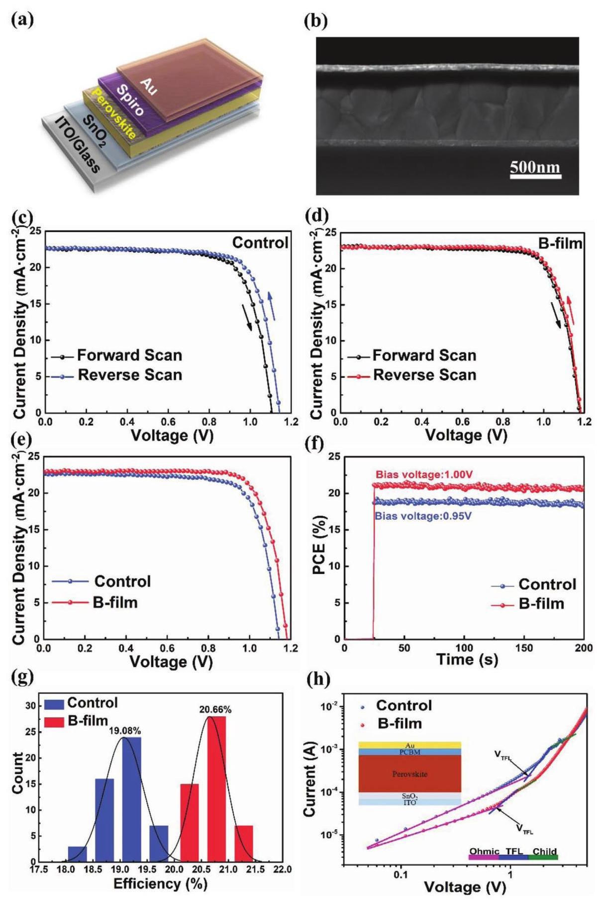
Figure 4. The J-V curves of devices. a) Illustration of the planar perovskite solar cell. b) Cross-sectional SEM image of the B-film device. c) Control device and d) B-film device with different scan directions. e) Control and B-film devices with reverse direction. f) Stabilized power output characteristics at the maximum power point of the control and B-film devices. g) Statistical results of the device performance. h) Dark I-V curves of the electron-only device revealing ${V}_{\text{ TFL }}$ kink point behavior.
Table 1. Summary of photovoltaic parameters for perovskite solar cells based control and B-film.
| Sample | Scan direction | ${V}_{\mathrm{{oc}}}\left\lbrack \mathrm{V}\right\rbrack$ | ${J}_{\mathrm{{sc}}}\left\lbrack {\mathrm{{mA}}{\mathrm{{cm}}}^{-2}}\right\rbrack$ | FF | PCE [%] | Steady-state output [%] |
| B-film | Reverse | 1.183 | 22.88 | 0.78 | 21.11 | 20.83 |
| Forward | 1.180 | 23.01 | 0.77 | 20.91 | ||
| Control | Reverse | 1.143 | 22.57 | 0.76 | 19.61 | 18.82 |
| Forward | 1.107 | 22.62 | 0.75 | 18.78 |
Supporting Information
Supporting Information is available from the Wiley Online Library or from the author.
Acknowledgements
Y.T. and X.Y. contributed equally to this work. This work was funded by the National Natural Science Foundation of China (Grant Nos. 91733301, 61722501, 91433203, 61377025, and U1705256), the 973 Program of China (Grant No. 2015CB932203), and the General Financial Grant from the China Postdoctoral Science Foundation (Grant No. 2017M620519).
Conflict of Interest
The authors declare no conflict of interest.
Keywords
defects, diboron, interface, perovskite solar cells, unreacted FAI
Received: August 5, 2018
Revised: August 31, 2018
Published online:
[1] A. Kojima, K. Teshima, Y. Shirai, T. Miyasaka, J. Am. Chem. Soc. 2009, 131, 6050.
[2] J. Burschka, N. Pellet, S. J. Moon, R. Humphry-Baker, P. Gao, M. K. Nazeeruddin, M. Gratzel, Nature 2013, 499, 316.
[3] A. Mei, X. Li, L. Liu, Z. Ku, T. Liu, Y. Rong, M. Xu, M. Hu, J. Chen, Y. Yang, M. Gratzel, H. Han, Science 2014, 345, 295.
[4] N. J. Jeon, J. H. Noh, W. S. Yang, Y. C. Kim, S. Ryu, J. Seo, S. I. Seok, Nature 2015, 517, 476.
[5] Z. Xiao, C. Bi, Y. Shao, Q. Dong, Q. Wang, Y. Yuan, C. Wang, Y. Gao, J. Huang, Energy Environ. Sci. 2014, 7, 2619.
[6] C. Wehrenfennig, G. E. Eperon, M. B. Johnston, H. J. Snaith, L. M. Herz, Adv. Mater. 2014, 26, 1584.
[7] Y. Tu, J. Wu, X. He, P. Guo, T. Wu, H. Luo, Q. Liu, Q. Wu, J. Lin, M. Huang, Z. Lan, S. Li, J. Mater. Chem. A 2017, 5, 21161.
[8] X. Zheng, B. Chen, J. Dai, Y. Fang, Y. Bai, Y. Lin, H. Wei, X. C. Zeng, J. Huang, Nat. Energy 2017, 2, 17102.
[9] Y. Wu, A. Islam, X. Yang, C. Qin, J. Liu, K. Zhang, W. Peng, L. Han, Energy Environ. Sci. 2014, 7, 2934.
[10] W. S. Yang, B. W. Park, E. H. Jung, N. J. Jeon, Y. C. Kim, D. U. Lee, S. S. Shin, J. Seo, E. K. Kim, J. H. Noh, S. I. Seok, Science 2017, 356, 1376.
[11] W. S. Yang, J. H. Noh, N. J. Jeon, Y. C. Kim, S. Ryu, J. Seo, S. I. Seok, Science 2015, 348, 1234.
[12] S. Pang, H. Hu, J. Zhang, S. Lv, Y. Yu, F. Wei, T. Qin, H. Xu, Z. Liu, G. Cui, Chem. Mater. 2014, 26, 1485.
[13] M. Saliba, T. Matsui, J. Y. Seo, K. Domanski, J. P. Correa-Baena, M. K. Nazeeruddin, S. M. Zakeeruddin, W. Tress, A. Abate, A. Hagfeldt, M. Gratzel, Energy Environ. Sci. 2016, 9, 1989.
[14] J. H. Noh, S. H. Im, J. H. Heo, T. N. Mandal, S. I. Seok, Nano Lett. 2013, 13, 1764.
[15] J. P. Correa-Baena, L. Steier, W. Tress, M. Saliba, S. Neutzner, T. Matsui, F. Giordano, T. J. Jacobsson, A. R. Srimath Kandada, S. M. Zakeeruddin, A. Petrozza, A. Abate, M. K. Nazeeruddin, M. Gratzel, A. Hagfeldt, Energy Environ. Sci. 2015, 8, 2928.
[16] E. H. Anaraki, A. Kermanpur, L. Steier, K. Domanski, T. Matsui, W. Tress, M. Saliba, A. Abate, M. Gratzel, A. Hagfeldt, J. P. Correa-Baena, Energy Environ. Sci. 2016, 9, 3128.
[17] K. Yan, M. Long, T. Zhang, Z. Wei, H. Chen, S. Yang, J. Xu, J. Am. Chem. Soc. 2015, 137, 4460.
[18] Q. Hu, L. Zhao, J. Wu, K. Gao, D. Luo, Y. Jiang, Z. Zhang, C. Zhu, E. Schaible, A. Hexemer, C. Wang, Y. Liu, W. Zhang, M. Gratzel, F. Liu, T. P. Russell, R. Zhu, Q. Gong, Nat. Commun. 2017, 8, 15688.
[19] B. Philippe, M. Saliba, J. P. Correa-Baena, U. B. Cappel, S. H. Turren-Cruz, M. Gratzel, A. Hagfeldt, H. Rensmo, Chem. Mater. 2017, 29, 3589.
[20] J. A. Christians, P. Schulz, J. S. Tinkham, T. H. Schloemer, S. P. Harvey, B. J. Tremolet de Villers, A. Sellinger, J. J. Berry, J. M. Luther, Nat. Energy 2018, 3, 68.
[21] T. J. Jacobsson, J. P. Correa-Baena, E. Halvani Anaraki, B. Philippe, S. D. Stranks, M. E. Bouduban, W. Tress, K. Schenk, J. Teuscher, J. E. Moser, H. Rensmo, A. Hagfeldt, J. Am. Chem. Soc. 2016, 138, 10331.
[22] Y. H. Lee, J. Luo, M. K. Son, P. Gao, K. T. Cho, J. Seo, S. M. Zakeeruddin, M. Gratzel, M. K. Nazeeruddin, Adv. Mater. 2016, 28, 3966.
[23] L. Wang, C. McCleese, A. Kovalsky, Y. Zhao, C. Burda, J. Am. Chem. Soc. 2014, 136, 12205.
[24] Q. Chen, H. Zhou, T. B. Song, S. Luo, Z. Hong, H. S. Duan, L. Dou, Y. Liu, Y. Yang, Nano Lett. 2014, 14, 4158.
[25] D. Bi, W. Tress, M. I. Dar, P. Gao, J. Luo, C. Renevier, K. Schenk, A. Abate, F. Giordano, J. P. Corra-Baena, J. D. Decoppet, S. M. Zakeeruddin, M. K. Nazeeruddin, M. Gratzel, A. Hagfeldt, Sci. Adv. 2016, 2, e1501170.
[26] S. Chen, X. Wen, J. S. Yun, S. Huang, M. Green, N. J. Jeon, W. S. Yang, J. H. Noh, J. Seo, S. I. Seok, A. Ho-Baillie, ACS Appl. Mater. Interfaces 2017, 9, 6072.
[27] H. J. Snaith, A. Abate, J. M. Ball, G. E. Eperon, T. Leijtens, N. K. Noel, S. D. Stranks, J. T. W. Wang, K. Wojciechowski, W. Zhang, J. Phys. Chem. Lett. 2014, 5, 1511.
[28] W. Zhang, S. Pathak, N. Sakai, T. Stergiopoulos, P. K. Nayak, N. K. Noel, A. A. Haghighirad, V. M. Burlakov, D. W. deQuilettes, A. Sadhanala, W. Li, L. Wang, D. S. Ginger, R. H. Friend, H. J. Snaith, Nat. Commun. 2015, 6, 10030.
[29] Y. J. Yoo, J. Hong, R. T. Hatch, Biotechnol. Bioeng. 1987, 30, 147.
[30] A. A. Petrov, E. A. Goodilin, A. B. Tarasov, V. A. Lazarenko, P. V. Dorovatovskii, V. N. Khrustalev, Acta Crystallogr. 2017, 73, 569.
[31] H. Li, W. Shi, W. Huang, E. P. Yao, J. Han, Z. Chen, S. Liu, Y. Shen, M. Wang, Y. Yang, Nano Lett. 2017, 17, 2328.
[32] F. Jiang, W. C. Choy, X. Li, D. Zhang, J. Cheng, Adv. Mater. 2015, 27, 2930.
[33] D. Luo, W. Yang, Z. Wang, A. Sadhanala, Q. Hu, R. Su, R. Shivanna, G. F. Trindade, J. F. Watts, Z. Xu, T. Liu, K. Chen, F. Ye, P. Wu, L. Zhao, J. Wu, Y. Tu, Y. Zhang, X. Yang, W. Zhang, R. H. Friend, Q. Gong, H. J. Snaith, R. Zhu, Science 2018, 360, 1442.
[34] D. Bi, A. M. El-Zohry, A. Hagfeldt, G. Boschloo, ACS Photonics 2015, 2, 589.
[35] C. Roldán-Carmona, P. Gratia, I. Zimmermann, G. Grancini, P. Gao, M. Graetzel, M. K. Nazeeruddin, Energy Environ. Sci. 2015, 8, 3550.
[36] N. J. Jeon, J. H. Noh, Y. C. Kim, W. S. Yang, S. Ryu, S. I. Seok, Nat. Mater. 2014, 13, 897.
[37] H. Zai, C. Zhu, H. Xie, Y. Zhao, C. Shi, Z. Chen, X. Ke, M. Sui, C. Chen, J. Hu, Q. Zhang, Y. Gao, H. Zhou, Y. Li, Q. Chen, ACS Energy Lett. 2018, 3, 30.
[38] D. Bi, C. Yi, J. Luo, J. D. Décoppet, F. Zhang, S. M. Zakeeruddin, X. Li, A. Hagfeldt, M. Gratzel, Nat. Energy 2016, 1, 16142.
[39] T. Niu, J. Lu, R. Munir, J. Li, D. Barrit, X. Zhang, H. Hu, Z. Yang, A. Amassian, K. Zhao, S. Liu, Adv. Mater. 2018, 30, 1706576.
[40] M. C. Kim, B. J. Kim, D. Y. Son, N. G. Park, H. S. Jung, M. Choi, Nano Lett. 2016, 16, 5756.
[41] J. Peng, Y. Wu, W. Ye, D. Jacobs, H. Shen, X. Fu, Y. Wan, T. Duong, N. Wu, C. Barugkin, H. Nguyen, D. Zhong, J. Li, T. Lu, Y. Liu, M. N. Lockrey, K. J. Weber, K. R. Catchpole, T. P. White, Energy Environ. Sci. 2017, 10, 1792.
[42] A. Baumann, K. Tvingstedt, M. Heiber, S. Väth, C. Momblona, H. Bolink, V. Dyakonov, APL Mater. 2014, 2, 081501.
[43] Y. Liu, Z. Yang, D. Cui, X. Ren, J. Sun, X. Liu, J. Zhang, Q. Wei, H. Fan, F. Yu, X. Zhang, C. Zhao, S. Liu, Adv. Mater. 2015, 27, 5176.
[44] Y. Zhao, H. Tan, H. Yuan, Z. Yang, J. Z. Fan, J. Kim, O. Voznyy, X. Gong, L. N. Quan, C. S. Tan, J. Hofkens, D. Yu, Q. Zhao, E. H. Sargent, Nat. Commun. 2018, 9, 1607.
[45] F. Cai, L. Yang, Y. Yan, J. Zhang, F. Qin, D. Liu, Y. B. Cheng, Y. Zhou, T. Wang, J. Mater. Chem. A 2017, 5, 9402.
[46] X. Zhang, X. Ren, B. Liu, R. Munir, X. Zhu, D. Yang, J. Li, Y. Liu, D. Smilgies, R. Li, Z. Yang, T. Niu, X. Wang, A. Amassian, K. Zhao, S. Liu, Energy Environ. Sci. 2017, 10, 2095.
[47] D. Yang, R. Yang, X. Ren, X. Zhu, Z. Yang, C. Li, S. Liu, Adv. Mater. 2016, 28, 5206.
[48] D. Luo, L. Zhao, J. Wu, Q. Hu, Y. Zhang, Z. Xu, Y. Liu, T. Liu, K. Chen, W. Yang, W. Zhang, R. Zhu, Q. Gong, Adv. Mater. 2017, 29, 1604758.